A multi-layer PCB (Multi-layer Printed Circuit Board) is a printed circuit board formed by laminating three or more layers of copper foil circuits alternately with insulating substrates. Electrical interconnections between layers are achieved through through-holes, buried vias, or blind vias. It serves as the core carrier enabling “high-density integration and complex functionality” in modern electronic devices, differing from single-layer/ dual-layer PCBs with only one or two circuit layers, enabling the placement of more components and signal traces within a limited space.

| Project | Parameter Range | Technical Advantages |
| Layer Count Range | 2-32 layers (including standard multilayer and high-density multilayer) | Covers the full spectrum of multilayer PCB requirements from basic to high-end, supporting complex interconnect designs |
| Minimum Line Width / Spacing | Standard Version: 3mil (0.076mm) High Precision Version: 2mil (0.05mm) | Meets high-density routing requirements, enhancing circuit integration |
| Board Thickness Range | 0.2mm–3.0mm | Accommodates structural space requirements for diverse devices, supporting ultra-thin/thickened customization |
| Via Specifications | Mechanical Vias: ≥0.15mm Laser Vias: ≥0.07mm | Compatible with buried/blind vias, through-holes, and other interconnect methods to optimize signal transmission paths |
| Substrate Types | FR4, High Tg FR4 (150℃+), Halogen-Free FR4, Metal-Clad, High-Frequency Substrates (PTFE), etc. | Suitable for general-purpose, high-temperature, eco-friendly, and high-frequency applications |
| Surface Finishes | Lead-free Hot Air Solder Leveling (HASL), Electrolytic Nickel Immersion Gold (ENIG), Electrolytic Nickel Immersion Silver, Electrolytic Nickel Immersion Tin, OSP, Gold Plating, etc. | Meets diverse soldering requirements, corrosion resistance, and electrical performance specifications |
| Maximum Processing Dimensions | 500mm × 600mm | Supports multilayer circuit demands for medium-to-large equipment |
Multilayer PCBs are printed circuit boards formed by alternately laminating multiple layers of insulating substrates with copper foil, achieving electrical interconnections between layers via through-holes, buried vias, or blind vias.
Key Differences from Single-Layer / Double-Layer PCBs
| Feature | Multi-Layer PCB | Single-Layer / Double-Layer PCB | Advantage |
| Routing Density | High (2-32 layers) | Low (1-2 layers only) | Supports higher component integration, reducing device size |
| Signal Processing Capability | Strong (interference resistance, low crosstalk) | Weak (prone to interference) | Suitable for high-frequency, high-speed, and complex signal systems |
| Mechanical Strength | High (multi-layer laminated structure) | Lower | Adaptable to industrial, automotive, and other vibration-prone environments |
| Application Scenarios | Complex electronic devices (e.g., motherboards, servers, industrial control hosts) | Simple circuits (e.g., remote controls, small sensors) | Meets core circuit requirements for mid-to-high-end electronic equipment |
Superior Technical Capabilities: Mastery of core manufacturing processes for 2-32 layer multilayer PCBs, expertise in critical technologies such as blind/buried vias, fine line patterns, and impedance control. Layer-to-layer alignment accuracy ≤±0.05mm, meeting high-density circuit requirements.
Stringent Quality Assurance: Strictly implements IPC-6012 Class 2/3 standards, establishes end-to-end quality control systems, sources premium materials from globally renowned brands (Jiantou, Shengyi, etc.), maintains exceptionally low defect rates, and holds ISO 9001, UL, RoHS certifications.
Rapid Delivery Capability: 48-hour express prototyping, 30% shorter lead times for bulk orders, and dedicated emergency order channels to align with customer product development and launch schedules.
Hassle-Free One-Stop Service: Comprehensive end-to-end solutions covering design, prototyping, mass production, assembly, and testing. This reduces supply chain management costs while providing full technical support and troubleshooting solutions.

Smartphone motherboards, laptop motherboards, tablets, smart TVs, router core boards

Automation controllers, robot control units, industrial power supplies, PLCs (Programmable Logic Controllers)

5G base station modules, switches, optical communication equipment, RF circuits

In-vehicle infotainment systems, ECUs (Electronic Control Units), sensor modules, battery management systems (BMS) for new energy vehicles

Medical imaging equipment (CT, ultrasound), portable monitors, surgical instrument control boards

Satellite communication equipment, spacecraft control systems, solar inverters, energy storage device circuits
PCBWDX, a leading Chinese manufacturer of multilayer PCBs, provides global customers with comprehensive multilayer circuit solutions, guided by the principles of “technology as the core, quality as the foundation, and service as the bridge.” Whether it’s high-density motherboards for consumer electronics, high-stability controllers for industrial control, or high-reliability control units for automotive electronics, PCBWDX’s superior manufacturing capabilities, rigorous quality control, and efficient delivery help customers stand out in the market, making it a reliable partner for electronic equipment manufacturers.


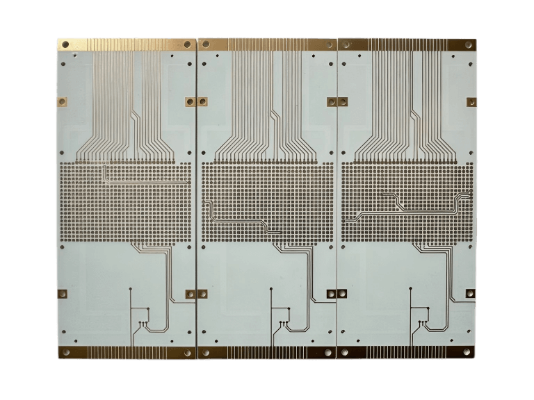
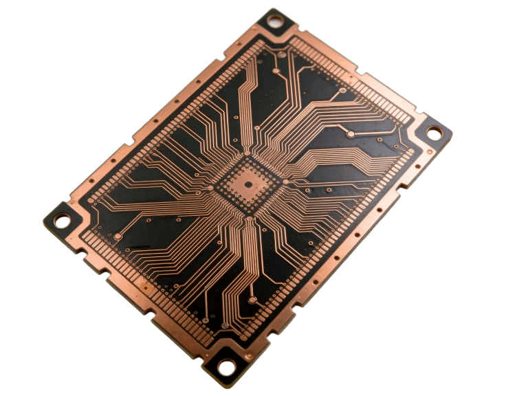

The stacking principle of single-layer, double-layer, and Multilayer PCBs involves alternately pressing together multiple layers of copper foil (signal layers, power layers, ground planes) and insulating dielectric layers (such as FR-4) to form a single unit, with vias providing electrical connections between layers. Single-layer PCBs have only one layer of copper foil, with all components located on the same side; double-layer PCBs have two layers of copper foil with an insulating layer in between; Multilayer PCBs typically consist of inner layers (signal/power/ground) and outer layers (signal/silkscreen). The more layers, the more flexible the routing and the better the performance.
The most direct way to distinguish between single-layer and multi-layer PCBs is to look at the number of circuit layers, light transmission, and the metallization of the drilled holes: single-layer boards have only one layer of copper foil, with circuits on only one side; multi-layer boards are opaque when viewed against light; the vias in multi-layer boards usually have copper (metallized holes) for inter-layer connections, while the holes in single-layer boards are non-metallized. Multi-layer boards are manufactured by pressing together inner layers, resulting in higher circuit density and more complex structures.
Inter-layer insulation and bonding are achieved through prepreg (pre-impregnated material).
The conventional number of layers is 4-16, but in special applications (such as servers), it can reach over 50 layers.
Single-layer PCBs have limited circuit layout capabilities, while Multilayer PCBs can implement more complex circuits and reduce electromagnetic interference.
Multilayer PCBs are widely used because they can achieve higher density and more functions in a smaller space, while providing better electrical performance, signal integrity, heat dissipation, and mechanical strength. This meets the urgent needs of modern electronic devices for miniaturization, high performance, and high reliability, and they are widely used in mobile phones, computers, communications, automobiles, and other fields.
The absence of three-layer PCBs is mainly due to unstable manufacturing processes, low cost-effectiveness, and warping issues. The PCB manufacturing industry typically uses an even number of layers (such as four or six layers) to ensure symmetry. Even if a three-layer function is required, it will be designed as a “fake” four-layer board, adding a blank layer or ground layer in the middle to ensure manufacturing stability and product quality.
