

A six-up production panel shipped from the PCBWDX line at a measured 0.600 mm. Green solder mask, white legend, gold-plated contact pads at both ends, UL 94V-0 and RoHS. This is what happens between the Gerber file and the carton.
Most buyers read a PCB datasheet from the top down. The hard engineering lives in the middle.
Layers, trace width, target impedance — those are the easy rows. The difficult part of a job like this one is holding a 0.6 mm core flat through plating, keeping gold contact pads contactable after years of insertion cycles, and yielding six clean boards from a process window thinner than a credit card.
The panel shown here is a long, narrow SMT assembly carrier built around gold-plated contact pads at both ends, with controlled serpentine routing on the back. It left the line at 0.600 mm finished thickness, verified by digital micrometer at the edge.
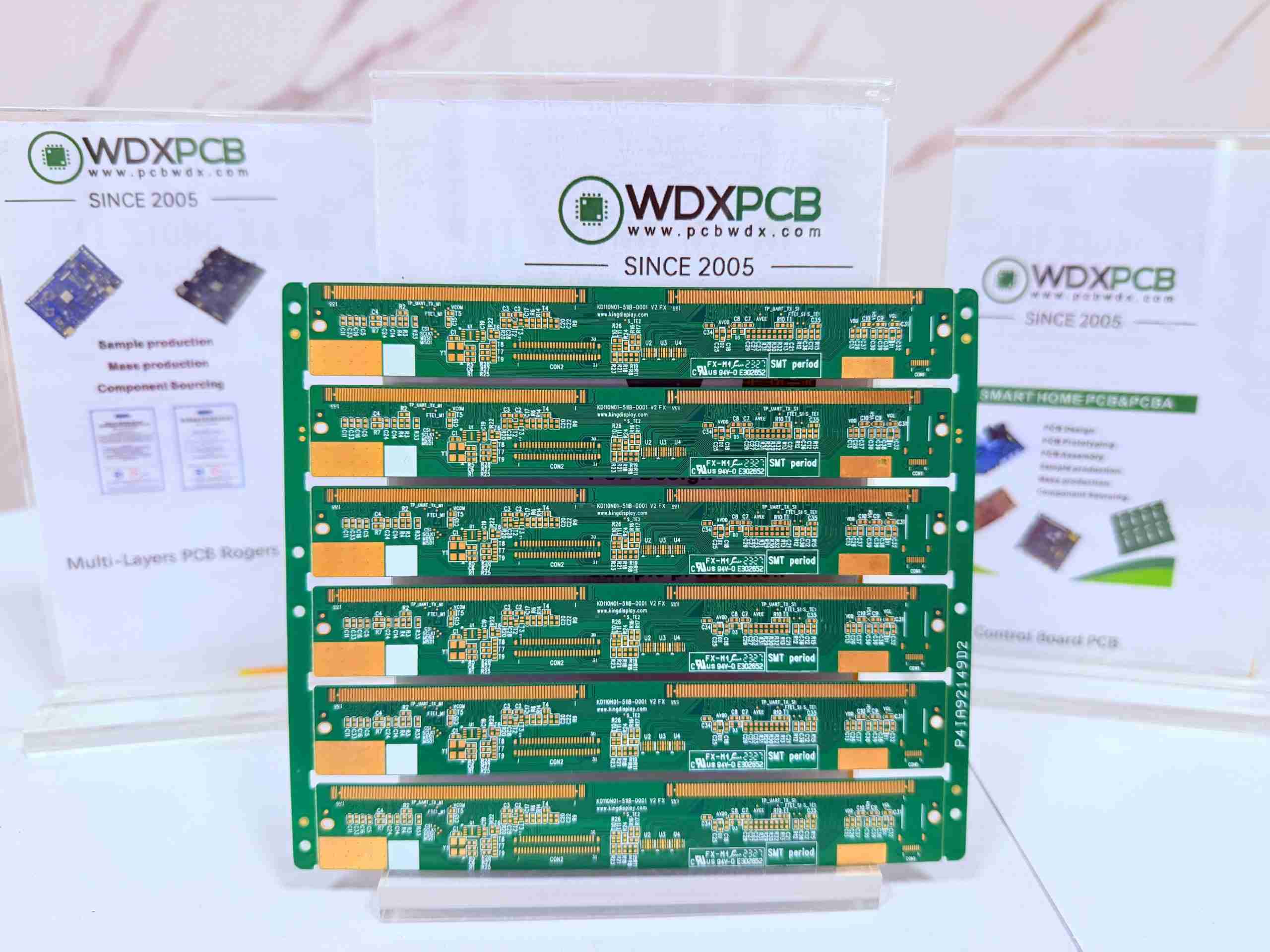
FIG. 01 · FRONT / COMPONENT SIDE
Six identical boards panelized on a common rail. SMT pads, gold contact areas, white silkscreen, RoHS 94V-0 marking and panel serial visible.

FIG. 02 · BACK / SOLDER SIDE
Fine trace routing with impedance-controlled serpentines, gold pads at both ends, mounting holes along the rails.

FIG. 03 · INCOMING QC
Digital micrometer reading 0.600 mm at the board edge. Finished thickness is measured, not estimated from the lamination recipe.
What the panel is built to.
| FINISHEDBOARDTHICKNESS | 0.6 mm-measured 0.600 mm at QC |
| SOLDER MASK | Green, LPI (liquid photoimageable) |
| LEGEND | White, component designators and compliance marks |
| SURFACE FINISH | Gold plating on contact pad windows; mask elsewhere |
| SMT COMPATIBILITY | Reflow-ready paste-printed pads, panel-level tooling holes |
| PANELIZATION | 6-up array on routing rails, depaneled after assembly |
| FLAMMABILITY | UL 94V -0 (E302092 marking on board) |
| COMPLIANCE | ROHS |
| PRODUCTION SCOPE | Prototype, sample and mass production runs |
Eight steps from copper-clad core to shipped panel.
A 0.6 mm board is not a 1.6 mm board scaled down. Every station in the line has a narrower process window, and every station has to hold it.
Material selection and lamination
The copper-clad core arrives near the final thickness, so lamination pressure, temperature and cooling ramp are tuned to keep the panel flat. A 0.6 mm core that bows 0.5 mm across its width will not print paste, will not reflow flat, and will not seat a connector.
Drilling
Drilling a thin, flexible stack is a different problem than drilling a 1.6 mm board. Feed rate, spindle speed and drill wear are adjusted to the thinner stack to avoid nail-heading and exit burr on the back.
Electroless copper and panel plating
Hole walls must be copper-plated through, and surface copper must reach target weight without over-plating the traces. On a thin board, plating stress itself is a known warp source — current density and barrel time are set to keep the panel flat through the cycle.
Imaging and etching
The outer-layer pattern is imaged, developed and etched. The back side of this panel is the result: fine traces, with controlled-impedance serpentines laid out to keep a long, narrow signal path in check end to end.
Gold plating on the contact windows
The contact pads at both ends are plated selectively. Gold is specified here for a reason: repeated insertion cycles, low contact resistance, and no oxide layer to scrub off. The rest of the board stays under solder mask; only the contact window sees gold.
Solder mask and legend
Green LPI mask is applied, cured, and the white legend prints designators, the UL 94V-0 and RoHS marks, SMT reflow-window markers, and the panel serial. The mask covers the traces; the gold windows stay open for contact.
Routing and panelization
Six boards stay on a common rail with tooling holes along the edges, so the SMT line can hold the panel, print paste, place parts and reflow as one unit. Depanelization happens after assembly — that is the point of shipping a six-up panel instead of six loose boards.
E-test, AOI and thickness QC
Every panel goes through electrical net testing, automated optical inspection, and a mechanical thickness check. The micrometer reading on this job — 0.600 mm — is written into the outgoing QC report, not estimated from the lamination recipe.
Why 0.6 mm is a real trade-off, not a marketing line.
A 0.6 mm board is not a 1.6 mm board scaled down. Every station in the line has a narrower process window, and every station has to hold it.
Thinner flexes more. It also fits where 1.6 mm will not.
A standard 1.6 mm FR-4 board is the default because it is forgiving. A 0.6 mm board is not: it flexes more, it warps more easily during plating and reflow, and it has less copper to spread heat. What it buys you is an enclosure up to 60 % thinner, lower stack height inside a display or portable device, and less weight per unit. The trade-off is not a slogan — it is a process window that has to be held across drilling, plating, mask and routing, and verified at final QC.
Five applications a panel like this is built for.
APP 01
Display & LCD interface carriers
Long, narrow form factor with gold contacts at both ends is a classic display-link layout between a main board and the panel.
APP 02
Smart-home control panels
Space-constrained enclosures where 0.6 mm stack height saves millimeters inside a wall plate or touch controller.
APP 03
Industrial HMI & keypad controllers
Gold-plated contacts survive repeated flex, connector and insertion cycles that finish like HASL would not.
APP 04
LED strip & signage controllers
Narrow carrier, long trace runs, controlled impedance serpentines for signal integrity along the strip.
APP 05
Portable & battery-powered devices
Thin core reduces overall device thickness and weight — the reason the 0.6 mm spec exists in the first place.
APP 06
Test fixtures & interposers
Gold contact windows on a thin, flat carrier are a natural fit for socketed test and interface applications.
The markings on the board are an audit trail, not decoration.
A buyer who knows what to look for can read compliance, process window and job identity directly off the white silkscreen.
- RoHS 94V-0 E302092
- RoHS-compliant material with a UL-listed 94V-0 flammability rating; the E-number is the UL file trace.
- SMT period
- Marks the reflow profile window for the SMT line — where the panel sits in the oven recipe.
- P41A9214902
- The panel serial. Ties this shipment back to the Gerber, stack-up and QC records for the job.
- CON2 / U3 / R26
- Reference designators for connectors and parts, printed for assembly and rework orientation.
Send the Gerber. Get the panel back.
PCBWDX has been manufacturing thin-core, gold-contact and multi-layer panels since 2005. Send the Gerber files plus the stack-up, surface finish and thickness requirements — prototypes in days, production panels in weeks.
About The Author
Betty Chen
Betty Chen has rich hands-on experience in PCB & PCBA industry. She focuses on PCB design, fabrication, SMT assembly, testing and reliability improvement. She shares practical technical insights of PCB manufacturing and assembly through articles.